Shenzhen Yideyi Technology Co., Ltd is a professional PCB
manufacturer, which is located in Shenzhen, China. After many years
development, it has become a company which integrates research &
development, reverse engineering,manufacture, SMT and sales.
What is Reverse engineering?
Reverse engineering, sometimes called back engineering, is a
process in which software, machines, aircraft, architectural
structures and other products are deconstructed to extract design
information from them. Often, reverse engineering involves
deconstructing individual components of larger products. The
reverse engineering process enables you to determine how a part was
designed so that you can recreate it. Companies often use this
approach when purchasing a replacement part from an original
equipment manufacturer (OEM) is not an option.
The reverse engineering process is named as such because it
involves working backward through the original design process.
However, you often have limited knowledge about the engineering
methods that went into creating the product. Therefore, the
challenge is to gain a working knowledge of the original design by
disassembling the product piece-by-piece or layer-by-layer.
Companies often use reverse engineering on old electronic
components, such as discontinued printed circuit boards (PCBs) and
connecting cards. Frequently, the products in question will come
from manufacturers that have since gone out of business. If the
manufacturer is still in business, they might no longer offer the
part. The firms often reverse engineer old electronics for the sake
of continuity.
In some cases, the only way to obtain the design of an original
product is through reverse engineering. With some older products
that have not been manufactured for 20 years or more, the original
2D drawings are no longer available.
Unique Niche
Our systems are a critical component to the hardware support
strategy for numerous military, governmental, aerospace, nuclear,
utility, automotive and commercial firms. They rely on our system
to keep their mission-critical hardware operational each and every
day.
Unique Technology
Internally developed software coupled with our low-cost vision
platform and NIST certified calibration equipment ensures that our
system is a solution that is custom tailored for your application.
Our hardware and software have been specifically designed to
maintain an excellent price-performance ratio, maximize your ROI
and provide a unique set of tools for effective and efficient
reverse engineering, regardless of the scale of your project.
Unique Process
Over our 10 years in business, we have continuously improved our
process to support cutting edge technology. Whether a circuit card
has two or twelve layers, blind or buried vias, and the substrate
is FR4 or Thermount, we have the process knowledge to ensure your
success.
How PCB Reverse Engineering Would Help PCB Design & Development?
PCB reverse engineering is a reverse research technology that uses
a series of reverse research techniques to obtain a PCB design,
circuit schematic and a BOM for an existing & matual electronic
design. A new product development that used to take two or three
years to develop, now through reverse engineering technolgy, may
take only a few months to complete.
Why Use Our PCB Reverse Engineering Service?
Our Reverse Engineering Services are designed + developed in
accordance with what you want and need. These services are widely
appreciated by our clients for their timely execution and genuine
prices.
1. Manufactured items are frequently smaller + more efficient —
saving you space, time, + costs.
2. All reverse engineering projects use only modern + current
components making any future repairs they may need easier + cost
effective.
3. Most units are upgradeable — we can add functionality, outputs,
sensors, or change programs slightly to broaden your processing
capability and to improve operations, maintenance + support issues
on older circuit Boards
4. Migration from through hole parts to SMD (Surface Mount Device)
parts
5. Migration to emerging technologies while retaining the core
features and logic of existing systems
6. Discover product strengths, weaknesses and limitations
7. To understand competitor's products and develop alternatives
8. Manufacturer of a product no longer exists or produces a product
9. Manufacturer of a product no longer supports/services a product
10. Documentation of the original design is lost or inadequate
11. To update obsolete components with current technology
12. Create better designs
PCB Reverse Engineering Services
We will reverse engineer your PCB sample, and submit the
engineering file into:
PCB Gerber File
BOM List
Schematic Diagram
YDY service:
1. PCBA, PCB assembly: SMT & PTH & BGA
2. PCBA and enclosure design
3. Components sourcing and purchasing
4. Quick prototyping
5. Plastic injection molding
6. Metal sheet stamping
7. Final assembly
8. Test: AOI, In-Circuit Test (ICT), Functional Test (FCT)
9. Custom clearance for material importing and product exporting
10. PCBA reverse engineering
11. Professtional R&D team
12. PCB Layout Design
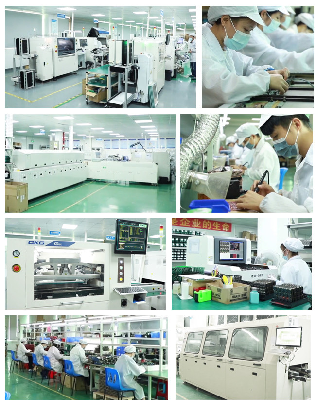
PCB Assembly Manufacturing Procedures:
Program Management
PCB Files → DCC → Program Organizing → Optimization → Checking
SMT Management
PCB Loader → Screen Printer → Checking → SMD Placement → Checking →
Air Reflow → Vision Inspection → AOI → Keeping
PCBA Management
THT→ Soldering Wave (Manual Welding) → Vision Inspection → ICT →
Flash → FCT → Checking → Package → Shipment
Each board is carefully examined by our dedicated inspection team
using AOI and high magnification viewers.
Using our X-Ray machine, we test PCBs to component level and all
wiring is fully inspected and tested. Flash
testing and earth bonding tests can also be undertaken where
required