Sign In | Join Free | My himfr.com
Home > Multilayer Printed Circuit Board >

16 Layer Multilayer Printed Circuit Board Assembly Buried Resistance

    Buy cheap 16 Layer Multilayer Printed Circuit Board Assembly Buried Resistance from wholesalers
     
    Buy cheap 16 Layer Multilayer Printed Circuit Board Assembly Buried Resistance from wholesalers
    • Buy cheap 16 Layer Multilayer Printed Circuit Board Assembly Buried Resistance from wholesalers
    • Buy cheap 16 Layer Multilayer Printed Circuit Board Assembly Buried Resistance from wholesalers
    • Buy cheap 16 Layer Multilayer Printed Circuit Board Assembly Buried Resistance from wholesalers

    16 Layer Multilayer Printed Circuit Board Assembly Buried Resistance

    Ask Lasest Price
    Brand Name : YDY
    Model Number : M-004
    Certification : ISO13485, IATF16949, ISO9001,IOS14001
    Price : Negotiable
    Payment Terms : L/C, D/A, D/P, T/T, Western Union, MoneyGram
    Supply Ability : 50000pcs/month
    Delivery Time : 1-10 working days
    • Product Details
    • Company Profile

    16 Layer Multilayer Printed Circuit Board Assembly Buried Resistance

    Buried Resistance Board PCBA Multilayer Printed Circuit Board Printed Wiring​


    Shenzhen Yideyi Technology Co., Ltd founded in 2008, It's an industry leading producing and R&D manufacturer in silk screen printing, gift and electronic areas with deep domain expertise and best service to help clients get high-quality and competitive products with 13 years history. Based on our professional and innovative technologies, we produce membrane switch, flexible circuit, membrane panel, lens, crystal epoxy, adhesive sticker, name plate and so on. In addition, there is an electronic department to produce various electronic products (eg. writing tablet, air purifier, mosquito killer, keyboards, Bluetooth speaker etc).

    Also, we have a gift department to produce various gifts (eg. acrylic ornament etc). Our products are widely used in electronic products, household appliances, toys, industry control equipments, medical equipments, telecommunication area, vehicle-mounted, lighting, instrument and apparatus, fitness equipments, power, mobile phone and so on, which have been widely exported to Europe, America, Japan and other countries, received praise from our clients.

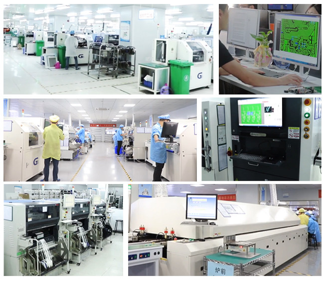
    There are more than 500 staffs in our factory with a variety of sophisticated high-end modern equipments, like all-auto silk-screen printer, semi-auto silk screen printer (15 sets), six-color printer, CNC engraving machine (25 sets), digital control cutting machines, laser cutter, injection molding machine, punching machine, etc.

    We also have dust-free workshop and labs, etc. There are many testing equipments in the labs, like binary tester,high and low temperature tester, tension tester, height tester, membrane switch life tester, membrane switch lead tester, etc. After several years' development and advancement, we've gained many achievements and certifications. Our company has passed ISO 9001:2008, ISO 14001:2004, OHSAS18001:2007, UL, SGS, TUV quality management system certification and other related product certifications (CE, FCC, RoHS, CCC, ASTM F963-16, etc).
    We attach great importance to win-win cooperation and focus on winning more value for our clients. "Continuous improving and serve for you with all sincerity" is our service tenet. You support is our developing dynamic and welcome your visit and guidance.


    More layers in a PCB board creates more surface area to run signal traces and power shapes to different devices. Very helpful considering how dense and power hungry most motherboards are. To this end, most motherboards have 8 to 10 layers for conventional designs.


    Our service


    1. SMT service;

    2. Design service, Gerber drawings;

    3. Good quality and fast delivery with lower price than double side PCB.

    4. Specifications of LEAD Free HASL 1 Layer / Single Side Rigid PCB/PCBA:


    1) Base material: FR-1(94v0), FR-4, CEM-1,

    2) Max Board size: 600*600mm

    3) Board thickness: 0.2mm/0.6mm/0.8mm/1.2mm/1.6mm/3.2mm

    4) Copper thickness: 0.5oz , 1oz , 2oz ,3oz,4oz, 5oz ,7oz , 11oz

    5) Special tech: BGA, PTH, Blind and buried vias

    6) Profile: V-scoring, V-cutting, punching, etching, milling, routing

    7) Surface treatment: HASL, OS, Immersion gold, gold plated (coating)

    8) With best price to USA, South American, India, South Africa and Europe

    9) Main market: USA, EGYPT, Europe, South American, mid-east

    10) Compliant: UL, ROHS, ISO9001-2000

    11) Standard: IPC-A-600F, IPC-D-300G, MIL-STD-105D LEVEL II

    12) Application: Home appliances, electronics, digital camera, LCD TV sets, medical equipments, telecommunication, LED lightings, street light, mobile phone, computer, laptop test equipment and power meter, electrical weighing scale, night

    13) Small quantity and prototypes acceptable

    14) Lead time: 5-7days for prototypes, 9-13days for mass production

    15) Available Service: OEM, 24hrs service for fast prototype


    Our Advantages:

    • Supply OEM/ODM and custom service
    • High quality with smart balance function
    • Wholesale price
    • ISO9001/ISO14001/CE/ROHS certificates
    • Fast delivery
    • Green product
    • One year warranty
    • Excellent safety performance
    • Short circuit testing passed
    • Overcharge testing passed
    • Over discharge testing passed
    • Original imported :IC from Japan,MOS from USA,Components from Sumsang.
    • 1.2m drop testing passed
    • 100% testing
    • Support ODM & OEM services

    SMT Production processes:


    Material Receiving → IQC → Stock → Material to SMT → SMT Line Loading → Solder Paste/Glue Printing → Chip Mount → Reflow → 100% Visual Inspection → Automated Optical Inspection (AOI) → SMT QC Sampling → SMT Stock → Material to PTH → PTH Line Loading → Plated Through Hole → Wave Soldering → Touch Up → 100% Visual Inspection → PTH QC Sampling → In-Circuit Test (ICT) → Final Assembly → Functional Test (FCT) → Packing → OQC Sampling → Shipping


    PCB Assembly Manufacturing Procedures:

    Program Management


    PCB Files → DCC → Program Organizing → Optimization → Checking


    SMT Management

    PCB Loader → Screen Printer → Checking → SMD Placement → Checking → Air Reflow → Vision Inspection → AOI → Keeping


    PCBA Management

    THT→Soldering Wave (Manual Welding) → Vision Inspection → ICT → Flash → FCT → Checking → Package → Shipment


    Files Requested For Quote:


    In order to provide you with the most efficient and accurate quote on manufacturing the requested unit, we ask that you provide us with the following information:


    1. Gerber file,PCB file,Eagle file or CAD file are all acceptable

    2. A detailed bill of materials (BOM)

    3. Clear pictures of PCB or PCBA sample for us

    4. Quantity and delivery required

    5. Test method for PCBA to guarantee 100% good quality products.

    6. Schematics file for PCB design if need to do function test.

    7. A sample if available for better sourcing

    8. CAD files for enclosure manufacturing if required

    9. A complete wiring and assembly drawing showing any special assembly instructions if required


    PCB Capability


    ProcessItemMass production capability
    SMTPrintingMax PCB size900*600mm²
    Max PCB weight8kg
    Solder paste printing tolerance±25μm(6σ)
    System repeat calibration tolerance±10μm(6σ)
    Scraper pressure detectionpressure closed-loop control system
    SPIDetect Min BGA PAD to PAD distance100μm
    x-axis and Y-axis tolerance0.5μm
    False Rate≤0.1%
    MountComponent size0.3*0.15 mm²--200*125 mm²
    Component max height25.4mm
    BGA/CSP Min PAD spacing, and Min PAD diameter0.30mm,0.15mm
    Populate tolerance±22μm(3σ),±0.05°(3σ)
    PCB board size50*50 mm²-850*560 mm²
    PCB thickness0.3mm--6mm
    Populate Max components type500
    AOIDetect Min components01005
    Detect false typeIncorrect conponents,missing components,opposite direction,,component shift,Tombstone,Mounting on side,unsoldering,insufficient solder,Lead raised,Solder ball
    Foot warping detection3D Detection function
    ReflowTemperature Accuracy±1ºC
    Welding protectionnitrogen protection;(remaining oxygen<3000ppm)
    Nitrogen ControlNitrogen closed-loop control system,±200ppm
    3D X-RayMagnificationGeometric Magnification;:2000 times;System Magnification:12000times
    Resolution1μm /nm
    Rotation Angle &Slanting PerspectiveAny ±45°+360°rotation
    DIPPreelaborationAutomatic forming technologyComponent Automatic forming
    DIPDIP technologyAutomatic Insertion machine
    Wave solderingWave soldering typeOrdinary wave soldering
    Inclination angle of transport guide rail4--7°
    Temperature accuracy±3ºC
    Soldering protectionnitrogen protection
    Non-welding pressure contact technologyMax PCB board size800*600mm²
    Press down height accuracy±0.02mm
    Pressure Range0-50KN
    Pressure AccuracyStandard value:±2%
    Hold time0-9.999S
    Conformal coating technologyMax PCB board size500*475*6mm
    Max PCB board weight5kg
    Other characteristicConformal coating pressure Programmable control
    ICT testtest levelDevice level test,Test hardware connection status.
    Test point>4096
    Test contentContact test ,Open/short test,Resistance capacitance test test,diode, triode,mosfet test,No power on hybrid test,Boundary scan chain test,Power on mixed mode test.

    16 Layer Multilayer Printed Circuit Board Assembly Buried Resistance


    Trade Terms:


    1. Payment: T/T in advance (Western Union , paypal is welcomed)


    2. Production lead time 100PCS: 5-7days, 500~1000PCS: 7-10days, above 1000PCS 15-20days.


    3. Sample can be delivered in 3days


    4. Shipping freight are quoted under your requests


    5. Shipping port: Shen zhen,Mainland China


    6. Discounts are offered based on order quantities


    7. MOQ: 1PCS


    Package &Shipping Methods:


    1. Vacuum package with silica gel, Carton box with packing belt.

    2. By DHL, UPS, FedEx, TNT

    3. By EMS

    4. By sea for mass quantity according to customer's requirement


    We are the smart choice for you and the trusted source at the center of your deal. Welcome the win-win situation together.

    16 Layer Multilayer Printed Circuit Board Assembly Buried Resistance


    pcba application:

    16 Layer Multilayer Printed Circuit Board Assembly Buried Resistance


    FAQ:


    Q1. How to keep our product information and design file secret ?
    We are willing to sign a NDA effect by customers side local law and promising to keep customers data in high confidential level.


    Q2. What file formats do you accept for production?

    Gerber file: CAM350 RS274X

    PCB file: Protel 99SE, P-CAD 2001 PCB

    BOM: Excel (PDF,word,txt)


    Q3. Please note that the following detail will speed up evaluation:
    Material:
    Board thickness:
    Copper thickness:Surface finish:
    Solder mask color:
    Silkscreen color:


    Q4. How to make sure the PCBAs are completely well recieved?
    We will pack with aluminum bag, and insert card, up and bottom card with stable cartons.

    Q5. How to ship the PCBAs?
    For small packages, we will ship the boards to you by DHL,UPS,FEDEX,TNT. Door to door service! For mass production, we could ship by air, by sea.


    Q6. How to make sure the function is fine?
    We could make sample/prototype and do functional testing before mass production.


    Quality 16 Layer Multilayer Printed Circuit Board Assembly Buried Resistance for sale
    Inquiry Cart 0
    Send your message to this supplier
     
    *From:
    *To: Shenzhen Yideyi Technology Limited Company
    *Subject:
    *Message:
    Characters Remaining: (0/3000)